
LM358 IC – The Versatile Dual Operational Amplifier
The LM358 is a widely-used dual operational amplifier (op-amp) IC that plays a crucial role in analog circuit design. Known for its low power consumption and ease of use, it is an essential component in signal amplification, filtering, and other analog applications. Let's dive into its construction, working principles, applications, and example projects.
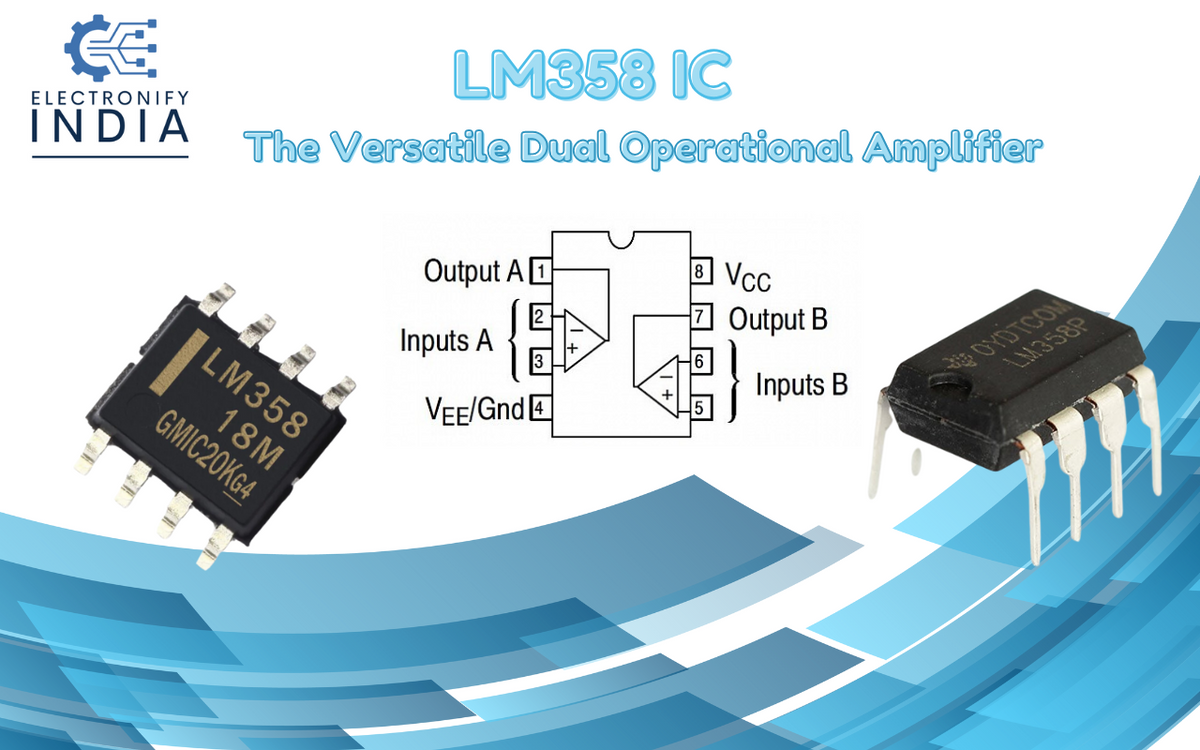
Construction and Internal Design

The LM358 consists of two independent, high-gain op-amps in an 8-pin DIP (Dual In-line Package) or SMD (Surface Mount Device) form. Each op-amp has three terminals – inverting input (-), non-inverting input (+), and output. Internally, the IC uses bipolar junction transistors (BJTs) for high performance and stability. It operates efficiently with a single power supply, making it ideal for battery-powered and portable devices.
Working Principle
The LM358 amplifies the voltage difference between its inverting and non-inverting inputs. The amplified output can drive other components in the circuit. Its low input bias current ensures minimal interference with sensor outputs, while the high gain allows for significant signal amplification. The LM358 can operate with a single power supply ranging from 3V to 32V or a dual supply of ±1.5V to ±16V, providing flexibility in design.
Applications
- Signal Amplification: Used to boost weak signals from sensors and transducers.
- Comparators: Compares input voltages for control applications.
- Active Filters: Creates low-pass, high-pass, and band-pass filters.
- Voltage Followers (Buffers): Prevents circuit loading.
- Oscillators and Waveform Generators: Generates signals for timing and wave-shaping circuits.
- Current-to-Voltage Converters: Converts sensor output into readable voltage levels.
Specifications
- Voltage Supply: 3V to 32V (single supply) or ±1.5V to ±16V (dual supply)
- Bandwidth: 1 MHz
- Slew Rate: 0.3 V/μs
- Input Bias Current: 45 nA
- Operating Temperature: 0°C to 70°C
Example Projects
Temperature Control Using LM358 and Thermistor

In this circuit, a 100k NTC thermistor is connected to a 5V power supply on one end, while the other end is linked to a 10k potentiometer (P1). The wiper (middle pin) of P1 is connected to the inverting input (pin 2) of the LM358 operational amplifier. As the temperature rises, the resistance of the NTC thermistor decreases, causing the voltage at pin 2 to increase.
The non-inverting input (pin 3) of the LM358 is connected to the wiper of another 10k potentiometer (P2), with its two ends connected to 5V and ground (GND). This potentiometer acts as a voltage divider, allowing you to set the reference voltage for temperature control.
When the circuit is powered on, the voltage at pin 2 is initially lower than at pin 3, resulting in a high output from the LM358. This activates the relay, starting the heating process.
As heating progresses, the thermistor’s resistance drops, increasing the voltage at pin 2. When this voltage surpasses the level at pin 3, the output of the LM358 switches low, turning off the relay and stopping the heating.
Once the heating stops, the thermistor cools, increasing its resistance and causing the voltage at pin 2 to drop. When the voltage at pin 2 falls below pin 3’s reference voltage, the output goes high again, restarting the heating. This cycle repeats continuously to maintain temperature regulation.
Role of P1 (Potentiometer 1)
The 10k potentiometer (P1) is used to calibrate the temperature threshold. By adjusting P1, you can fine-tune the circuit to achieve precise temperature control.
Output Circuit Explanation
The output circuit uses an S8050 NPN transistor. The base of the transistor connects to the LM358 output through a 10k resistor (R1), which limits the current. A 100k pull-down resistor (R2) is connected between the transistor’s base and ground to prevent false triggering when the LM358 output is low.
The collector of the transistor is connected to the 5V power supply via a 5V relay, while the emitter is grounded. A 1N4007 diode is placed across the relay terminals to protect the circuit from voltage spikes caused by relay switching (flyback voltage).
Key Considerations
This simple temperature control circuit, powered by the LM358, offers reliable performance and easy calibration. However, extra caution should be taken when dealing with high voltages (230V) to ensure safety during operation.
Auto Cut-off Circuit for Battery Charging Using LM358 IC

An automatic cut-off battery charging circuit is essential to prevent overcharging and extend battery life. This design uses the LM358 operational amplifier (op-amp) to monitor the battery voltage and disconnect the charger once the battery reaches a specified voltage level. The circuit is simple, efficient, and cost-effective.
Circuit Description and Working
In this circuit, the LM358 functions as a voltage comparator. One input monitors the battery voltage, while the other sets a reference threshold using a potentiometer. When the battery voltage exceeds the reference level, the charger is disconnected automatically.
Components Required
- LM358 Dual Operational Amplifier IC
- 5V Power Supply
- 12V Relay
- 1N4007 Diode
- 10k Potentiometer (P1, P2)
- BC547 NPN Transistor
- 100k NTC Thermistor (Optional for temperature sensing)
- 10k Resistors (R1, R3)
- 100k Resistor (R2)
- Battery (12V)
Construction and Connections
- Voltage Sensing: The battery's positive terminal is connected to one end of a 10k potentiometer (P1). The wiper of P1 is connected to the inverting input (pin 2) of the LM358.
- Reference Voltage: Another 10k potentiometer (P2) is used as a voltage divider. Its wiper is connected to the non-inverting input (pin 3) of the LM358, while the two ends are connected to 5V and ground, respectively.
- Comparator Action: When the battery voltage (pin 2) is lower than the reference voltage (pin 3), the output at pin 1 is high, activating the relay and allowing charging.
- Auto Cut-Off: When the battery is fully charged and its voltage exceeds the reference voltage, the output at pin 1 switches low, deactivating the relay and disconnecting the charger.
Output Circuit
- Transistor Switching: The output of the LM358 is connected to the base of a BC547 NPN transistor through a 10k resistor (R1). A 100k pull-down resistor (R2) ensures the transistor remains off when the LM358 output is low.
- Relay Control: The transistor’s collector connects to the relay, while the emitter is grounded. A 1N4007 diode is placed across the relay to suppress voltage spikes.
How It Works
- When the battery voltage is low, the LM358 output is high, so the relay is turned on and the charging process starts.
- As the battery charges, the voltage at pin 2 rises.
- Once the battery voltage exceeds the threshold set by P2, the LM358 output goes low, switching off the relay and stopping the charging.
- This cycle repeats, ensuring the battery is not overcharged.
Applications
- Battery backup systems
- Portable power banks
- Solar battery chargers
- Automotive battery chargers
Benefits
- Prevents Overcharging: Automatically disconnects the charger when the battery is full.
- Simple and Low-Cost Design: Uses minimal components and is easy to construct..
Why Choose LM358?
The LM358 is cost-effective, widely available, and reliable for various applications. Its ability to operate with a single supply and handle low-voltage signals makes it indispensable in analog circuit design. Whether you are building simple circuits or complex systems, the LM358 provides the performance and flexibility needed to enhance your projects. For more information check datasheet.
Get best price for LM358 IC and also Explore our range of Integrated circuits at ElectronifyIndia.com for your next electronic design project!
